Application & Results
A selection of numerous high quality results obtained with UNISOKU systems. Most of the excellent pieces of work have been provided by customers to whom we express our acknowledgement of gratitude.
UHV Low Temperature JT-SPM
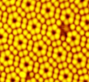
STM measurements on Au(111) @ 1.2 K
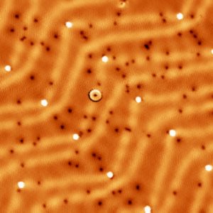
STM Topography
54nm x 54nm
Herringbone structure
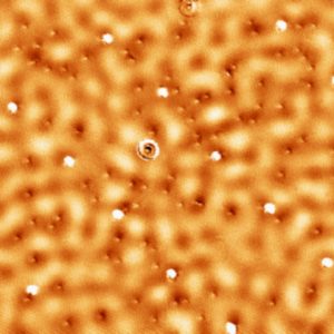
Spectroscopy
di/dv image resolving the surface state
images by courtesy of SPECS GmbH, Berlin
STM on K2PTCDA Molecules on Ag(111)
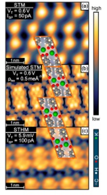
a)* STM image with a tungsten tip
b) _Calculated STM image for comparison
c)* ST[H]M image by applying the “Hydrogen STM” method reveals even more detail of the molecular structure
)* Courtesy of Christian Zwick and Torsten Fritz, Friedrich Schiller University Jena
Published in ACS Nano, 2016 Jan 26. [Epub ahead of print http://www.ncbi.nlm.nih.gov/pubmed/26718635]
Complex Stoichiometry-Dependent Reordering of 3,4,9,10-Perylenetetracarboxylic Dianhydride on Ag(111) upon K Intercalation, C.Zwick, A.Baby, M.Gruenewald, E.Verwüster, O.T.Hofmann, R.Forker, G.Fratesi, G.P.Brivio, E.Zojer, and T.Fritz
Reproduced under Creative Commons Attribution (CC-BY) License
http://pubs.acs.org/page/policy/authorchoice_ccby_termsofuse.html
High Performance AFM on Au(111)
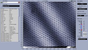
Non-contact AFM topography
High scan speed 16nm/s
Multi Mode Non-Contact AFM
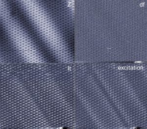
AFM regulated on df = const.
Scan speed 16nm/s
Z topographic channel
df error signal
It simultaneous tunnelling current map
and simultaneous excitation signal map
images by courtesy of SPECS GmbH, Berlin
UHV LT STM System USM1200
STM Topographic Image of Si (100)
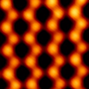
Temperature: 63K
Field of View: 3nm × 3nm
Dr. YOKOYAMA
in Yokohama city Univ.
STM Molecular Structure and Topographic Image of COOH-Porphyrin-tetramer
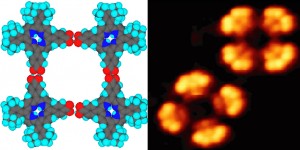
Temperature: 63K
Field of View: 11nm × 11nm
Dr. YOKOYAMA
in Yokohama city Univ.
back to the instrument USM1200
UHV ULT and High Magnetic Field STM System USM1300
3D Vector Magnet Application:
Spin Transitions of a Single Fe Atom
STM at 500mK on single Fe atoms on a Cu2N layer on Cu(100)
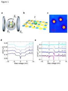
IETSpectra at magnetic fields of 0T and 2T along the symmetry axes reveal the spin transitions of a single Fe atom.
(step position corresponds to excitation energy; step height to the intensity of the transition)
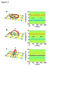
left: depicts the rotation plane of the field vector;
right: excitation energy vs. angle of rotation.
Colour indicates intensity:
strong asymmetry in the yz-plane
no asymmetry in the xy-plane.
The asymmetric behaviour of the spin states relates to the direction of the neighbouring N-atoms.
Courtesy of Sebastian Loth, Max Planck Institute for Structure + Dynamics of Matter, Hamburg.
Three-Dimensional Mapping of Single-Atom Magnetic Anisotropy
Shichao Yan et al. Nano Lett. (2015), 15, 1938−1942
http://pubs.acs.org/doi/abs/10.1021/nl504779p
STM Topographic Image of Vortex Lattice of a Superconductor NbSe2
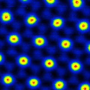
Temperature: 400mK
Field: 0.5T
Environment: UHV
Field of View: 250nm × 250nm
Dr. HANAGURI
in Magnetic Materials Laboratory, RIKEN
STM Topographic Image and STS Data of Cleaved NBS2
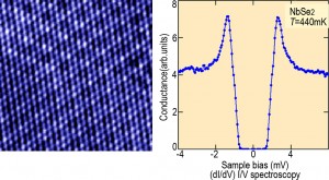
Temperature: 440mK
Field of View: 7.3nm × 7.3nm
Dr. HANAGURI
in Magnetic Materials Laboratory, RIKEN
STM topographic image in 11Tesla at 400mK by USM1300S 3He
Scan size: 11.7nm
Sample bias: 2.07V
Tunnel current: 740pA
Si (001) STM topographic image by USM1300S 3He
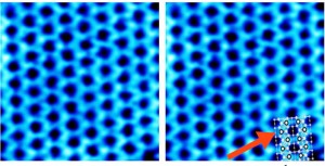
Add the atomic structure model
N type Si (100), 0.008 ~ 0.015Ωcm
V=+1.7V, I=70pA, 668.7mK
Keisuke Sagisaka, NIMS, Fujita group
published in VOLUME 91, NUMBER 14, 146103, PHYSICAL REVIEW LETTERS
Standing wave on Cu (111) surface by USM1300
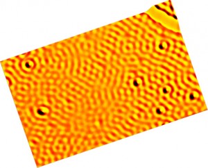
Yukio Hasegawa group
Univ. of Tokyo, Solid state physics
back to the instrument USM1300
UHV LT SPM System USM1400
Naphthalene Molecules on HOPG: Tunneling Spectroscopy
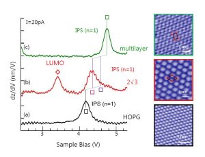
a) HOPG substrate
b) (2√3×2√3) R30° Naphthalene layer
c) Multilayer of Naphthalene
Osaka University
T. Yamada et al, J. of Phys. Chem. C 118,1045 (2014)
http://pubs.acs.org/doi/abs/10.1021/jp4097875
STM Topographic Image of Si (111) Surface
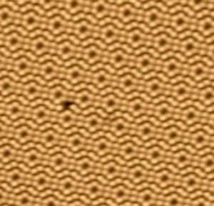
Temperature: 83K
Scan area: 22nm × 22nm
Sample bias: 1.8V
Tunnel current: 0.54nA
Yuko Yamamoto
Unisoku Co., Ltd.
STM Topographic Image of Si(100) Surface

Temperature: 83K
Scan area: 12nm × 5nm
Sample bias: 1.2V
Tunnel current: 1.0nA
Yuko Yamamoto
Unisoku Co., Ltd.
back to the instrument USM1400
UHV LT-SPM and Raman System USM1400-TERS
Tip Enhanced Raman Spectroscopy (TERS)
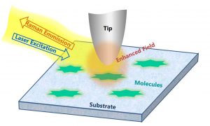
Experimental set up
Intensity enhancement by near-field effect
Single Molecule TERS Spectra
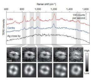
Local Raman Spectroscopy
top: spectra of a single H2TBPP molecule
middle: spatial distribution of spectral band
bottom: calculated spatial distribution
Z.C. Dong (Hefei National Laboratory for Physical Sciences at the Microscale)
Nature 498, 82–86 (06 June 2013) doi:10.1038/nature12151
http://www.nature.com/nature/journal/v498/n7452/full/nature12151.html
Proof of Single Molecule Resolution
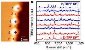
Left: STM topographic image of an alternating chain of ZnTBPP (red) and H2TBPP (blue) molecules on Ag
Right: local Raman spectra at the locations as indicated by the numbers revealing a clear separation between neighbouring molecules.
Spectra at top and bottom labelled with DFT are calculated for comparison
S.Jiang + Z.C.Dong et al Nature Nanotechnology 10, 865–869 (2015)
http://www.nature.com/nnano/journal/v10/n10/abs/nnano.2015.170.html
back to the instrument USM1400-TERS
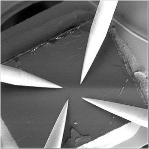
Low Temperature 4-probe System USM1400-4P
4 point measurement
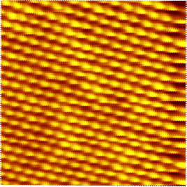
STM image on HOPG at 6.5K
back to the instrument USM1400-4P
4-Nano-Probe System for SEM UMP-1000
Four probes over carbon nanotube
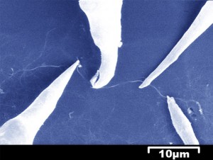
Four-terminal Resistance measuremaent on Carbon NanotubeProbe distance: <10μm
Prof. Sumiyama
Nagoya Institure of Technology
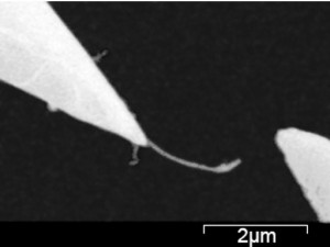
Cutting CNT by 2 probes
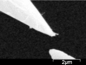
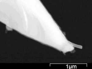
Applying a voltage across the probes
M. Yoshimura, Ueda Lab., Toyota Technological Institute

